Quantitative CL Uniquely Resolves Individual Point Defects in InGaN/GaN Quantum Wells, Solving Efficiency Gain Riddle
Crystallographic point defects (PDs) can act as non-radiative recombination centres in InGaN quantum wells (QWs). They have been shown to significantly reduce the emission efficiency of photonic devices. Thanks to the high spatial resolution provided by the Attolight Allalin SEM-CL system, individual PDs embedded in the QWs can be characterized. By combining image processing and temperature-dependent measurements, different types of PDs can be distinguished. The resulting insights enable the tailoring of sample design and material growth conditions for efficient InGaN-based optoelectronic devices.
In commercial InGaN/GaN-based lightemitting devices (LEDs), an indium-containing underlayer (UL) is typicallygrown before the InGaN quantum well (QW) to significantly improve emissionefficiency. However, whilethecritical role of the UL hasbeen identified decades ago, its role has only recently been understood; it capturescrystallographic point defects (PDs) before they migrate into the QW, reducingnon-radiative centres in the active region [1]. These defects originate fromnitrogen vacancies formed during high-temperature GaN buffer-layer growth [2,3],a step common to all MOVPE/MOCVD-grown GaN-based samples. If designed adequately, the UL can effectively suppress such defects by trapping themwith indium atoms. Poorly engineered ULs allow defects to migrate into the QW,severely quenching light emission. Because these PDs occur at the atomic scaleand are buried within indium-containing layers, they have largely beenoverlooked; conventional structural inspection tools such as AFM, SEM, and TEMcannot readily detect them. Quantitative cathodoluminescence is the only tool that enables rapidPD detection and therefore UL engineering for best QW performance.
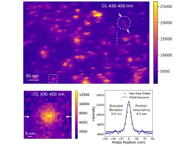
Since PDs act as non-radiative centresin InGaN layers, their presence can, in principle, be inferred optically. Themain limitation, however, is the required spatial resolution. Typical PDdensities in QWs often exceed 109 cm-2 [4,5], which correspond to an average PD spacing of roughly 300 nm or less. This rules outdetection by standard optical characterization techniques, likephotoluminescence, whose spatial resolution is limited to hundreds ofnanometers at best. SEM-CL, in contrast, uses a focused electron beam toachieve nanometre-scale excitation, making it ideally suited for imagingindividual PDs in InGaN QWs.
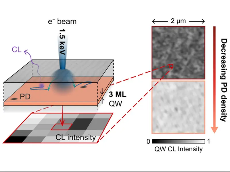
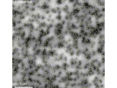
In a recent study from the Ecole PolytechniqueFédérale de Lausanne (EPFL) using an Attolight Allalin system, individual PDsin a 3 monolayer (ML) thick QW were clearly resolved by applying a low-energyelectron beam of 1.5 keV at a sample temperature of 10 K [6] (Fig. 1). Using sucha low electron beam energy, the interaction volume within the sample issignificantly reduced, while the cryogenic temperature helps minimize thecarrier diffusion length in the QW. Together, these factors achieve a spatialresolution of approximately 80 nm in the CL intensity map, enabling theisolation of individual PDs in the QW.
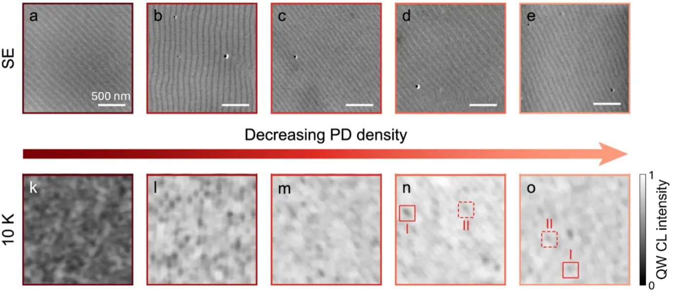
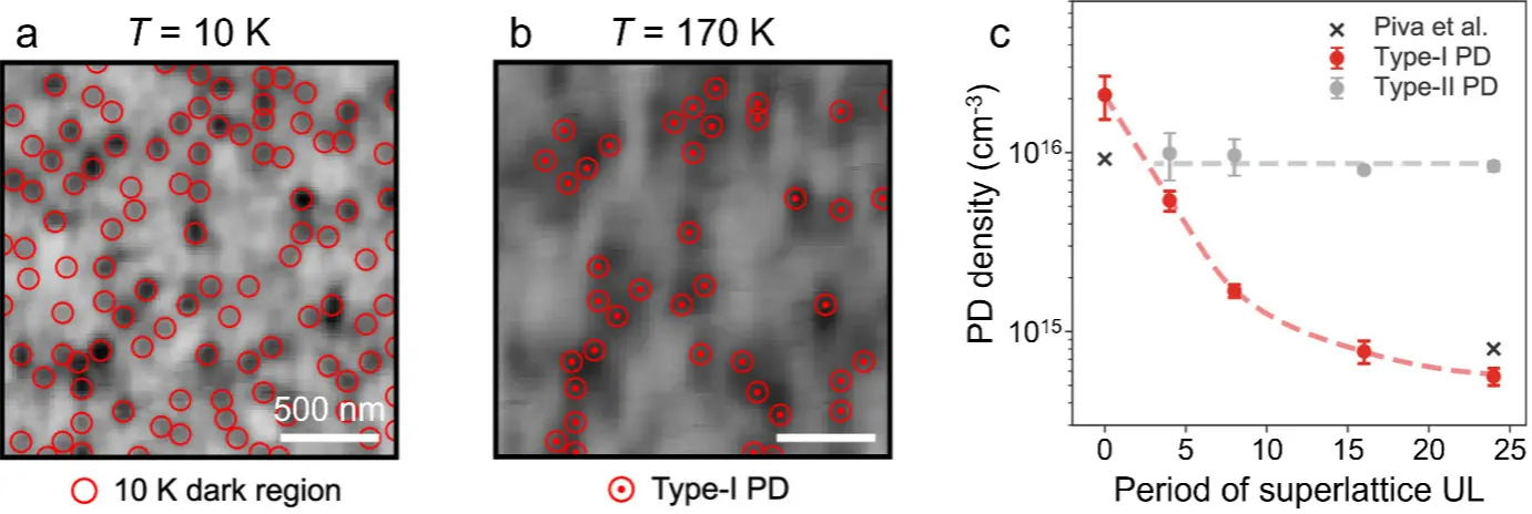
Temperature-dependent CLmeasurements were performed on the same sample areas, revealing two distincttypes of PDs. Both types are visible at 10 K; however, type-I PDs continue tostrongly affect emission at 170 K, while type-II PDs nearly disappear at highertemperatures (Figs. 2a & 2b). By tuning the number of PD-related non-radiativecentres in the QW through variation of the indium-containing UL structure, thedensity of type-I PDs observed in CL intensity maps changes, whereas type-II PDdensity remains constant (Fig. 2c). These results indicate that the detrimentaldefects responsible for quenching QW emission at room temperature are type-IPDs, which can be effectively suppressed through careful design of the ULstructure.
Conclusion
This study highlights the critical role of crystallographic point defects in determining the performance of InGaN-based light-emitting devices and demonstrates the power of nanoscale-resolution SEM-CL for identifying the corresponding non-radiative channels in the active region. Such atomic-level insights provide important guidance for refining growth strategies and boosting the efficiency of photonic devices based on InGaN/GaN quantum wells.
[1] C. Haller et al., Appl.Phys. Lett. 113, 111106 (2018).
[2] Y. Chen et al., Appl.Phys. Lett. 118, 111102 (2021).
[3] A. Toschi et al., APLMater. 13, 031111 (2025).
[4] F. Piva et al., J.Phys. D: Appl. Phys. 54, 025108 (2021).
[5] C. Haller, “Elucidating therole of the InGaN UL in the efficiency of InGaN based light emitting diodes” (EPFL,Lausanne, Switzerland, 2019).
[6] T. F. K. Weatherley et al.,Nano Lett. 21, 12, 5217–5224 (2021).
Further reading
T. F. K. Weatherley, “Thenanoscale impact of individual nonradiative point defects on InGaN/GaN quantumwells” (EPFL, Lausanne, Switzerland, 2023).

More applications
Identifying Atomic-Scale Defects Responsible for Blue Emission in hBN Using Correlative STEM-CL
.webp)
Cathodoluminescence Analysis of Extra-Cellular Matrix
CL from Beam-Sensitive Optoelectronic Materials - Hybrid Halide Perovskites
Applications on Defect Visualization and Counting in Optoelectronic Materials
Applications on Semiconducting Diamond
