Resolving Picosecond Carrier Dynamics at the Nanoscale — The Attolight Allalin Chronos TRCL Solution
.webp)
Many critical processes happen before nanoseconds even start. In the picosecond to nanosecond timescale, luminescence experiments capture fast relaxation and initial recombination dynamics: formation and fast decay of excitons, fast energy transfer, and vibrational relaxation. This time domain is frequently used to study dominant recombination pathways in semiconductors, providing key metrics for assessing material quality and device performance — insights that are critical for advanced materials research, next-generation transistors, high-efficiency LEDs, emerging AI hardware, and other cutting-edge semiconductor technologies.
Overcoming the Sub-10 ps Measurement Challenge
GaN, one of the mostwell-known wide-bandgap semiconductors, exhibits ultrafast initial exciton formation and relaxation dynamics in the sub-picosecond range. However, the luminescence rise time for time-resolved photoluminescence (TRPL) in high-quality pure GaN is often reported in the range of 10-100 ps, limited by the instrument response function.
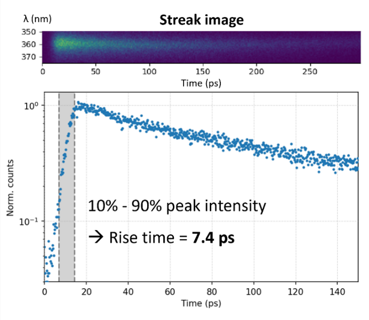
In fact, measuring sub-10 ps rise times is technically very challenging: it requires a pulse dexcitation source and detector with minimal jitter, as well as high signal-to-noise ratio to capture the fastest dynamics. With our time-resolved cathodoluminescence (TRCL) system using an ultrafast pulsed laser (pulse duration ~3 ps) and a ps-resolution streak camera, we can reliably measure rise times below 10 ps (Figure 1), which clearly demonstrates the high temporal resolution of the entire TRCL system and provides the precision needed to resolve most ps-scale carrier dynamics in luminescence experiments.
Preserving Nanoscale Spatial Resolution (< 15 nm)
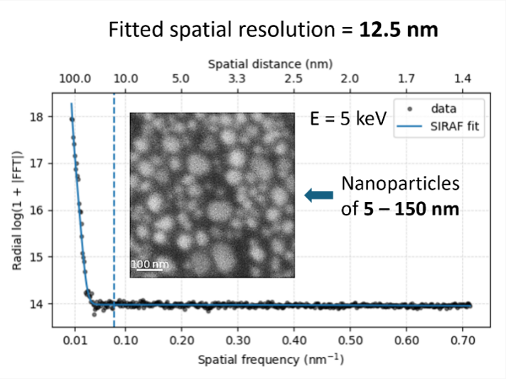
While exploring physicsat the picosecond timescale with high temporal resolution, we preserve nanoscale spatial resolution even in pulsed mode, achieving <15 nm resolution with a laser-pulsed electron beam (Figure 2). This maintains the key advantage of CL over PL: excitation beyond the diffraction limit. With such high spatial resolution, nanoscale structural features observed in scanning electron microscopy (SEM) can be directly correlated with TRCL through hyperspectral imaging, providing rich and comprehensive information in a single experiment.
Ease of Use and Actionable Data Extraction
With such rich and high-dimensional information contained in a single hyperspectral dataset, a key practical question is how to efficiently extract the most relevant insights.
To address this, our company provides dedicated support through a professional applications team,including skilled Python developers (contributors to the well-known HyperSpy package [2]), experienced experimentalists with over 15 years of expertise across all TRCL configurations—including beam blanker [3], laser-pulse dexcitation [4], time-correlated single photon counting (TCSPC) [5],second-order intensity correlation function (g²) measurements [6], pump-probe CL spectroscopy [7] and various streak camera systems [8]—and material scientists with strong backgrounds in both TRPL and TRCL on emerging semiconductor systems.
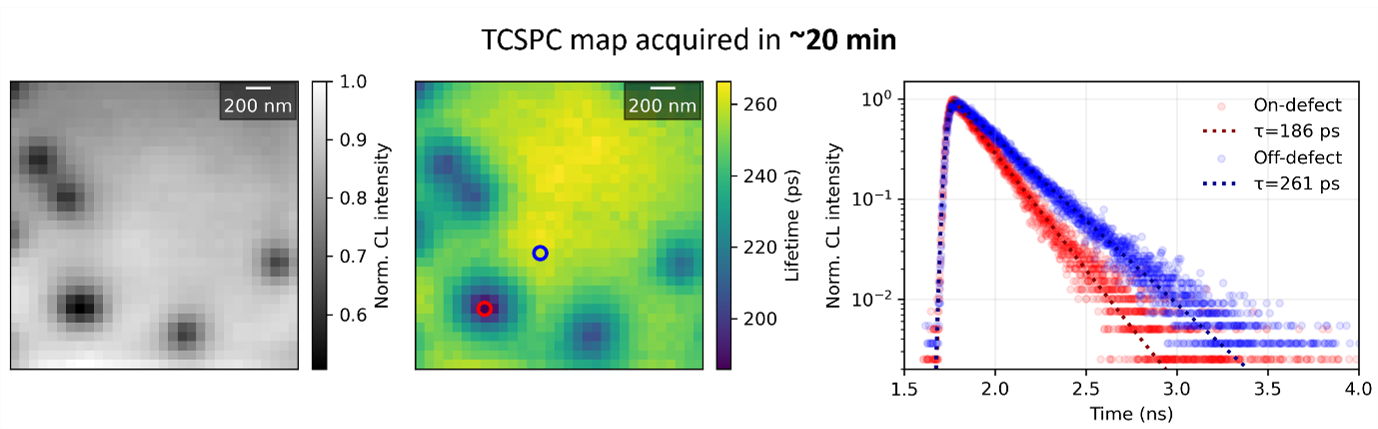
In addition, our user community has developed and shared a variety of advanced data processing approaches, enabling rapid extraction of key information—such as carrier lifetime maps (Figure 3), dopant concentration maps [9], and defect-related signatures (Figure 3) [10, 11]—within seconds to minutes. Based on your specific requirements, we further develop tailored analysis workflows to accelerate your data processing and unlock the full potential of TRCL measurements.
[1] Anders Brostrøm and Kristian Mølhave, Microsc Microanal. 2022 Mar 3:1-9.doi:10.1017/S1431927622000228.
[2] Francisco de la Peña,Eric Prestat, Jonas Lähnemann, Vidar Tonaas Fauske, Pierre Burdet, Petras Jokubauskas, Tom Furnival, Carter Francis, Magnus Nord, Tomas Ostasevicius, Katherine E. MacArthur, Duncan N. Johnstone, Mike Sarahan, Thomas Aarholt, Joshua Taillon, pquinn-dls, Vadim Migunov, Alberto Eljarrat, Jan Caron, … pietsjoh.(2026). hyperspy/hyperspy: v2.4.0 (v2.4.0). Zenodo.doi:10.5281/zenodo.18379337.
[3] https://www.attolight.com/products-options/beam-blanker
[4] https://www.attolight.com/products-options/ps-photoelectric-pulsed-source
[5] https://www.attolight.com/products-options/time-correlated-single-photon-counting-hybrid-photodetector
[6] https://www.attolight.com/technologies/cathodoluminescence-g2-autocorrelation
[7] https://www.attolight.com/products-options/streak-camera
[8] Magdalena Solà-Garcia, Sophie Meuret, Toon Coenen and Albert Polman, ACS Photonics. 2019, 7(1), 232-240. doi: 10.1021/acsphotonics.9b01463
[9] Nicolas Tappy, Pascal Gallo, Anna Fontcuberta i Morral and Christian Monachon, Carbon 191 (2022)48-54. doi: 10.1016/j.carbon.2022.01.030
[10] Thomas Weatherley,Gunnar Kusch, Duncan TL Alexander, Rachel A Oliver, Jean-François Carlin, Raphaël Butté and Nicolas Grandjean, Gallium Nitride Materials and Devices XIX,PC1288618 (2024). doi:10.1117/12.3000482
[11] Wei Liu, Jean-François Carlin, Nicolas Grandjean, Benoît Deveaud and Gwénolé Jacopin, Appl. Phys. Lett. 109, 042101(2016). doi:10.1063/1.4959832

More applications
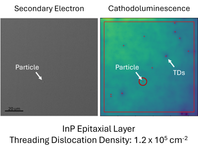
Cathodoluminescence as a Reliable Method to Quantify Threading Dislocations in InP-Based Optical Devices
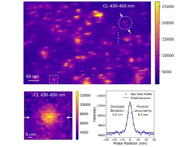
Identifying Atomic-Scale Defects Responsible for Blue Emission in hBN Using Correlative STEM-CL

Quantitative CL Uniquely Resolves Individual Point Defects in InGaN/GaN Quantum Wells, Solving Efficiency Gain Riddle
.webp)
Cathodoluminescence Analysis of Extra-Cellular Matrix
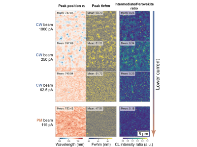
CL from Beam-Sensitive Optoelectronic Materials - Hybrid Halide Perovskites